
International Technology Roadmaps: The U.S. Semiconductor Experience
W. J. Spencer and T. E. Seidel
International SEMATECH
INTRODUCTION
“It is difficult to predict, especially the future!”
—Ancient Chinese Proverb
The semiconductor industry was born in 1947 with the invention of the point contact transistor on germanium material. The industry got a tremendous impetus to its growth with the development of the integrated circuit (IC) in the late 1950s. Germanium was replaced by silicon, and the technology to manufacture hundreds of millions of individual components on silicon microchips has led to a worldwide industry that will exceed $135 billion in sales in 1995. The semiconductor industry has undergone a compound annual growth rate of over 15 percent for several decades. The worldwide growth of the industry exceeded 25 percent per year in 1993 and 1994; it is expected to do the same in 1995.
The reason that the semiconductor industry has grown so dramatically—and is in fact the economic driving force for the Information Age—is a year-over-year increase in productivity of 25 to 30 percent. This productivity increase has been going on for nearly three decades and shows up as either a 30-percent-per-year reduction in cost of components on silicon or a 30-percent-per-year increase in the complexity of functions that can be performed in silicon. This productivity improvement is demonstrated clearly in the continual decrease in cost of semiconductor memory from the first introduction of 1,000-bit chips in around 1970 to today’s production of 4- and 16-megabit dynamic random access memories (DRAMs), and it is expected to continue well into the twenty-first century (see Figure 1).

FIGURE 1 Dynamic RAM Best-Bit Prices.
SOURCE: ICE and National Technology Roadmap.
There appear to be no major physical limitations to improving productivity in silicon integrated circuits for the next 15 to 20 years. Today’s 16-megabit DRAMs and associated microprocessor and logic chips are manufactured using 0.5-μm technology. The manufacturing facilities currently under construction will produce 0.35-μm and 0.25-μm products before the end of the decade. Table 1 shows a summary of the technologies projected by the National Technology Roadmap for Semiconductors (“Roadmap”) out through the year 2007. Behind this projection for the technology for the next 15 years are complete roadmaps for each of the major technologies in support of the manufacture of silicon integrated circuits. This work was the result of hundreds of scientists and engineers from universities, industry, and government working together to develop a set of industry requirements for silicon technology. The history of this roadmap process, the methods used to develop the National Technology Roadmap for Semiconductors, some of the overall requirements of the Roadmap, and finally, some sugges-
TABLE 1 Overall Roadmap Technology Characteristics
|
|
1992 |
1995 |
1998 |
2001 |
2004 |
2007 |
|
Feature Size (μm) |
0.5 |
0.35 |
0.25 |
0.18 |
0.12 |
0.10 |
|
Gate/chip |
300K |
800K |
2Mb |
5Mb |
10Mb |
20Mb |
|
Bits/chip |
|
|||||
|
—DRAM |
16Mb |
64Mb |
256Mb |
1Gb |
4Gb |
16Gb |
|
—SRAM |
4Mb |
16Mb |
64Mb |
256Mb |
1Gb |
4Gb |
|
Wafer processing cost ($/cm2) |
$4.00 |
$3.90 |
$3.80 |
$3.70 |
$3.60 |
$3.50 |
|
Chip size (mm2 ) |
|
|||||
|
—logic/μprocessor |
250 |
400 |
600 |
800 |
1000 |
1250 |
|
—DRAM |
132 |
200 |
320 |
500 |
700 |
1000 |
|
Wafer diameter (mm) |
200 |
200 |
200/400 |
200-400 |
200-400 |
200-400 |
tions for international cooperation and roadmaps in other technologies are the subject of this paper.
Technology roadmaps are not new to the semiconductor industry. The first semiconductor technology roadmaps were developed by SEMATECH in 1987. Earlier technology predictions were developed by the National Academy of Sciences’ Committee on Science and Public Policy (COSEPUP). Studies were initiated by COSEPUP in the early 1960s. In 1968 Philip Handler, who was then the President of the National Academy of Sciences, edited a book entitled Biology and the Future of Man.1 A survey of physics was done by the National Research Council under the chairmanship of George E. Pake in 1966.2 This study was updated in 19723 and again in 1986.4 Today, to the author’s knowledge, there is no plan to further update these surveys of fundamental science.
EARLY SEMATECH ROADMAP
The early planning of SEMATECH was greatly influenced by a set of industry-wide roadmap workshops held from June 1987 through March 1988. The latter month was coincident with the consortium’s occupation of its Austin,
Texas, site. These early workshops were driven by a group of about 20 planners from the future member companies of SEMATECH; leaders included Turner Hasty, who was later to serve as Chief Operating Officer. The first “organizing” workshop was held in Monterey, California; it provided a global competitive overview and developed planning guidelines for additional technology roadmapping to reach a competitive technology position for U.S. semiconductor manufacturers by 1990-1993. The workshop also identified topics for about 30 detailed workshops. Workshop topics included Lithography, Manufacturing Systems, Thermal Processes, Implant, Etch, Deposition and Etch Technologies, Manufacturing Facilities, Packaging, Metrology, Silicon Epi, Robotics & Automation, Test, Cleaning, and Process Architecture.
The Lithography workshop recognized that new exposure-tool technology required long development times, so planning decisions had to be developed quickly to meet 1993 goals for 0.35 μm. However, a vision to extend I-line to 0.35 μm was not developed at this time; in fact, history has shown the industry only made that decision as late as 1994. This early Lithography workshop scoped a list of options that included 1 × X-ray for use at 0.35 μm. It also used a systems approach for each lithographic technology option, considering mask, resist, and metrology needs for various exposure technologies.
Among the identification of general needs were architectures for factory data systems, improvement of defect densities (100x improvement was called for for the 0.5-μm generation), equipment specifications (later this evolved into a qualification methodology), defect-detection/metrology needs, and improved manufacturing cycle time, equipment, and reliability.
Specific technology requirements in the important Interconnect area include the development of tungsten plugs, a comparison of metal-physical and vapor-deposition schemes, and the characterization of electromigration. At the 0.5-μm Process Architecture workshop, the vision was set for the need for planarization of interlevel dielectrics when more than two levels of metal were required. This had an early influence that drove SEMATECH’s focus on chemical-mechanical planarization.
The Process Architecture workshops not only set roadmap process requirements and options but also made some operational recommendations. They included an evolutionary migration from the 0.8-μm AT&T process (which was the process incubator for SEMATECH) to generic 0.5- to 0.35-μm processes and the recommendation to delay a 200-mm demonstration until 150-mm equipment was further qualified. SEMATECH ultimately developed its own 0.35-μm processes and demonstrated 200-mm tool performance on 0.35-μm technology by the end of 1993.
Many of the organizers and leaders of the early workshops later served SEMATECH in management or advisory roles. They included Belani (NSC), Castrucci (IBM), Dehmel (Intel), Ferrell (Motorola), Hanson (NSC), Hasty (TI), Mackiewicz (AT&T), Oberai (IBM), Reilly (IBM), Seidel (UC-Santa Barbara),

and Sinha (AT&T). These workshops provided the basis for SEMATECH’s first five-year operational plan. Figure 2 shows three components of the five-year plan: manpower, budget, and technology generations. The curve represents manpower and the bars represent the quarterly budget.
MICROTECH 2000—DEVELOP A 1-GIGABIT STATIC RANDOM ACCESS MEMORY CHIP BY 2000
The 100th Congress of the United States established a National Advisory Committee on Semiconductors (NACS) in 1988. This was part of a Semiconductor Research and Development Act. The objectives of the Presidential Committee were to “devise and promulgate a national semiconductor strategy.” The committee included leaders from both industry and government. Between 1989 and 1992 the NACS published a series of recommendations for strengthening the U.S. semiconductor industry, including the equipment and materials suppliers.5 These reports were submitted to the President of the United States and resulted in additional funding for R&D in the U.S. semiconductor industry, principally from the Department of Defense. In addition, the NACS convened several ad hoc working groups in markets, environment, and technology. The Technology Committee was chaired by Dr. John A. Armstrong, who was then Vice President for Science and Technology at the IBM Corporation.
In April 1991 the Technology Committee of NACS and the U.S. federal government, through the Office of Science and Technology Policy, co-sponsored a workshop at Research Triangle Park in North Carolina. Nearly 100 representatives of U.S. semiconductor manufacturers, equipment makers, research institutions, universities, materials suppliers, and the federal government participated in the workshop. The objectives of the workshop were “to determine if the MicroTech 2000 technical goal of developing a competitive 0.12 micron semiconductor manufacturing process ahead of current forecasts is feasible, to identify the most critical efforts that should be undertaken to develop the manufactur-
TABLE 2 Microtech 2000 Architecture Roadmap
|
Year Required |
1993 |
1996 |
1998 |
2000 |
|
|
SRAM |
|||
|
Maximum |
16Mb |
64Mb |
256Mb |
1Gb |
|
Minimum design rules (μm) |
0.35 |
0.25 |
0.18 |
0.12 |
|
Access time (ns) |
10 |
6 |
4 |
2.5 |
|
Burst clock (Mhz) |
100 |
300 |
500 |
1200 |
|
|
SYSTEM-ON-A-CHIP |
|||
|
Minimum design rules (μm) |
|
0.35 |
0.25 |
0.18 |
|
On-chip SRAM |
|
8Mb |
64Mb |
256Mb |
ing process and to produce engineering samples of a product using the process, and to determine when resources would have to be made available to reach the goal by the year 2000.”
The outcome of the workshop was a report to the full NACS in August 1991.6 The workshop met its goal of developing a technology roadmap that would advance semiconductor technology by roughly one generation by the year 2000. This would make possible the manufacture of a 1-Gigabit static random access memory (SRAM) chip in early production phase by that time frame. The architecture roadmap is shown in Table 2.
The workshop report received wide circulation, and a great deal of discussion, within the U.S semiconductor industry. There was a general sense that the technology could be accelerated. There was a question in the industry as to whether the economics of this acceleration were worthwhile.
The NACS was a three-year committee activity that ended in 1992. In 1991, in preparation for its final report, the NACS asked the U.S. Semiconductor Industry Association (SIA) to take over some of its activities, including the implementation of the MicroTech 2000 workshop report. The SIA formed a Technology Committee under the leadership of Dr. Gordon Moore, who was then Chairman of the Board at Intel Corporation. Several meetings and telephone discussions between Dr. Moore and one of the authors led to the formation of a group to update the MicroTech 2000 report in 1992.
SEMICONDUCTOR INDUSTRY ASSOCIATION 1992 ROADMAP
The SIA, recognizing the United States must maintain its leadership in the semiconductor industry, which is enabling for the Information Age, sponsored the 1992 Semiconductor Technology Workshop to develop a comprehensive 15-year roadmap. Unlike the MicroTech 2000 report, which set the challenges for a particular technology generation (1G SRAM) circa the year 2000, the 1992 Roadmap assessed the current status and then set down the needs for each of five succeeding generations, looking out 15 years from 1992, to 2007. It was also the first time that industry, government, and academia worked together and broadly contributed expertise and insights to the effort.
Gordon Moore, chair of the SIA Technology Committee and general chair of the workshop, provided the keynote address and the leadership to make the workshop a success. The organizational leadership for this meeting, provided by the Semiconductor Research Corporation (SRC) and SEMATECH, formed a variety of management committees. They included a Framework Committee (led by Oberai Industry) and a Steering Committee (Burger [SRC]); these were composed of membership from industry, academia, and government. A Technology Committee (chaired by Bill Howard) was also formed to coordinate the efforts of each of the Technical Working Groups (lithography, interconnect, etc.).
The process that the groups followed was to develop the Roadmap “strawman,” or draft, and iterate it with their individual committee members. A revised draft of the Roadmap was issued before the workshop, and the key issues were highlighted for review at the actual workshop.
The charter of the workshop was to evaluate likely progress in key areas relative to expected industry requirements and to identify resources that might best be used to ensure that the industry would have the necessary technology for success in competitive world markets. One underlying assumption of the Semiconductor Technology Roadmap is that it refers to mainstream silicon Complimentary Metal-Oxide Silicon (CMOS) technology and does not include nonsilicon technologies.
This workshop consisted of 11 Technical Working Groups (TWGs): Chip Design & Test, chaired by Richard Howard; Process Integration, chaired by Dirk Bartelink; Lithography, chaired by Gordon McMillan; Interconnect, chaired by Thomas Seidel; Materials & Bulk Processes, chaired by Dyer Matlock; Environment, Safety & Health, chaired by Phyllis Pei; Manufacturing Systems, chaired by Hal Bogardus; Manufacturing Facilities, chaired by Craig Schackleton; Process Device Structure/CAD, chaired by Don Scharfetter; Packaging, chaired by John Kelly; and Equipment Modeling & Design, chaired by Edward Hall.
Altogether there were about 200 participants in the three-day workshop, which was held in Irving, Texas, in November 1992. The format included a general session followed by breakout sessions that featured cross-coordination of information among various technical working groups. For example, it was neces-
TABLE 3 Cost Targets
sary for the Lithography group to communicate with Interconnect and with Materials & Bulk Processes. Joint and breakout sessions alternated until consensus was reached or the final joint general session was held, at which time there was debate in an open forum.
The working groups defined critical success factors and core competencies needed for progress. Common themes and elements led to the set of overall key challenges that is shown in Table 1. In this table, the progression of feature sizes and chip complexity follows historical trends. Entries are organized by date of introduction of production startup; however, some entries reflect attributes of each technology generation at maturity. These characteristics were starting points for working-group deliberations.
For the first time, an industry technical roadmapping process prioritized the “cost-to-produce” as a key metric. The cost/cm2 was taken as a benchmark metric against which budget targets were developed for the various fab production technologies. For example, lithography was allocated 35 percent of the total, multilevel metal and etch 25 percent, and so forth (see Table 3).
Technical characteristics of note are increasing logic complexity (gates/chip) and chip frequency and decreasing power-supply voltage. These specific characteristics set the vision for requirements for dynamic power for CMOS. They also set in place additional implications for engineering the capabilities to achieve or manage those requirements.
Many organizations have used the Roadmap to set up their own development plans, to prioritize investments, and to act as resource material for discussion of technology trends at various forums, including those of international character. In the United States, one of the most significant results of the workshop was to reinforce a culture of cooperation. The intent to renew the Roadmap on a periodic basis was established.
One of the key conclusions of the 1992 Roadmap was the recognition that the infrastructure was unbalanced in its investments among fab technologies and design, test, packaging, and Technology Computer Aided Design (TCAD). This conclusion influenced SEMATECH’s board of directors to order the startup of
these silicon-to-systems activities in 1993. Two documents were published in 1993 to represent the 1992 Roadmap: Semiconductor Technology Workshop Conclusions7 and Semiconductor Technology Workshop Working Group Reports.8,9 Those documents were published and provided worldwide on a cost-free basis.
1994 UPDATE
The success of the 1992 Roadmap prompted the renewal of the Roadmap in 1994. A central assumption of the 1994 process was that Moore’s Law (a 4x increase in complexity every three years) would again extend over the next 15 years. Many experts have challenged this assumption because maintaining the pace of technology and cost reduction is an exceedingly difficult task. Nonetheless, no expectation or algorithm for slowing was agreed upon, and the coordinating committee framed the workshop against extension of Moore’s Law. A 15-year outlook was again taken, this time reaching to 0.07-μm CMOS technology in 2010. A proof of concept exists for low-leakage CMOS transistors near a 0.07-μm gate length. There appears to be no fundamental limit to fabrication of quality 0.07-μm CMOS transistors.
Unlike during the first roadmapping exercise, the management committees were consolidated into one committee: the Roadmap Coordinating Group (RCG), which played the roles of the former Framework, Steering, and Technology committees. The RCG was chaired by Owen Williams (Motorola), while different members fulfilled a mentoring responsibility for the various working groups, and several members (Burger, Seidel, and Wollensen) owned the creation and iteration of the overall (framing) characteristics. The RCG owned communication to the TWGs and the SIA’s Technology Committee (see Figure 3).
Again, all sectors of the U.S. semiconductor technology base participated: industry, universities, and government organizations. The theme of the 1994 Roadmap became the creation of a cooperative culture that builds a sense of “urgency without crises.”
The 1994 workshop, a one-day meeting, was held in Boulder, Colorado. Almost 300 participants met in a format that was condensed because the prework was carried out in such a way as to reach consensus within the various Technical Working Groups before the meeting. The meeting was an open forum where each chair and co-chair presented their summary of the Roadmap and then the entire audience held open debate on the issues that the proposed Roadmap presented.
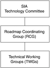
FIGURE 3 Roadmap coordinating committee structure.
In the 1994 workshop, there were only eight Technical Working Groups: Design & Test, chaired by R. Howard; Process Integration & Device Structure (PIDS), chaired by D. Bartelink; Environment, Safety & Health (ESH), chaired by R. Kirby; Lithography, chaired by G. McMillan; Interconnect, chaired by J. Martin; Materials & Bulk Processes (MBP), chaired by F. Robertson; Assembly & Packaging, chaired by A. Oscilowski; and Factory Integration, chaired by G. Gettel.
The consolidation of TCAD with PIDS and of Manufacturing Facilities, Manufacturing Systems, and Equipment Modeling & Design into Factory Integration accounts for the reduction from 11 groups in 1992 to eight. However, although it was recognized that Contamination-Free Engineering was a key part of MBP, all groups assessed contamination, materials, metrology, modeling, standards, and quality/reliability requirements. These latter technology areas cut across all eight technical working groups. The key summaries from each TWG are abstracted here:
-
Design & Test is dealing with an increase in complexity that threatens the ability to economically manage the design of higher complexity.
-
Process Integration & Device Structure is faced with power, performance, signal integrity, and complexity issues that require lower voltage, process simplification, and cross-functional coordination.
-
Environment, Safety & Health finds that future requirements mandate concurrent-engineering efforts to ensure ESH integrity (harmony with society).
-
Lithography forecasts the extension of optical technologies while predicting a future move to non-optical technologies, among which there is no preferred choice now.
-
Interconnect expresses needs in cost, density, performance, and reliability; this requires the engineering and integration of new materials and architectures, and a focus on productivity.
-
Materials & Bulk Processes is challenged by large wafers, thinner dielectrics, shallow junctions, process control, and contamination-free manufacturing.
-
Assembly & Packaging faces a variety of requirements paced by a proliferation of products in the market place but has special challenges in power and frequency requirements.
-
Factory Integration identifies productivity, complexity, flexibility, and cost as major issues.
The overall Roadmap characteristics in 1994 (see Table 4) were iterated with each of the TWGs and were developed in a self-consistent manner. The first three rows in the table are Major Market Product descriptions. The cost per function metrics for DRAM and microprocessors (μP) and the nonrecurring engineering cost for low-volume application-specific integrated circuits (ASICs) are listed. Similar overall characteristic charts include: number of Chip I/0s, number of wiring levels on chip (appropriate to Interconnect and Assembly & Packaging), defect density, mask count, wafer size (Factory Integration), power-supply voltage and maximum logic power (Process Integration & Device Structure and Design & Test).
In general, the trends between 1992 and 1994 overall characteristics are very similar. There is some acceleration in the migration to lower power supply voltage, and wafer size has now been standardized at 300 mm for the 0.18- to 0.13-μm generations.
The 1994 Roadmap has again been a useful vehicle for many forums. An electronic version has been piloted on the Internet, and there is discussion of renewal again in 1996 or 1997. One document was published in 1994, The National Technology Roadmap for Semiconductors,10 and again globally distributed.
INTERNATIONAL ROADMAPS
“If you don’t know where you’re going, any road will take you there.”
—Anonymous
The development of a National Technology Roadmap for Semiconductors has had a profound impact on semiconductor R&D in the United States. The Roadmap forms the basis for many technology discussions. The Roadmap results
TABLE 4 Overall Roadmap Technology Characteristics Major Markets
|
Year of First DRAM Shipment |
1995 |
1998 |
2001 |
2004 |
2007 |
2010 |
|
|
Minimum Feature Size (μm) |
0.35 |
0.25 |
0.18 |
0.13 |
0.10 |
0.07 |
Driver |
|
Memory |
|
D |
|||||
|
Bits/Chip (DRAM/Flash) |
64Mb |
256Mb |
1Gb |
4Gb |
16Gb |
64Gb |
|
|
Cost/Bit @ volume (millicents) |
0.017 |
0.007 |
0.003 |
0.001 |
0.0005 |
0.0002 |
|
|
Logic (High-Volume: Microprocessor) |
|
L (μP) |
|||||
|
Logic Transistors/cm2 (packed) |
4Mb |
7Mb |
13Mb |
25Mb |
50Mb |
90Mb |
|
|
Bits/cm2 (cache SRAM) |
2Mb |
6Mb |
20Mb |
50Mb |
100Mb |
300Mb |
|
|
Cost/Transistor @ volume (millicents) |
1 |
0.5 |
0.2 |
0.1 |
0.05 |
0.02 |
|
|
Logic (Low-Volume: ASIC) |
|
L (A) |
|||||
|
Transistors/cm2 (auto layout) |
2Mb |
4Mb |
7Mb |
12Mb |
25Mb |
40Mb |
|
|
Non-recurring engineering |
0.3 |
0.1 |
0.05 |
0.03 |
0.02 |
0.01 |
|
|
Cost/Transistor (millicents) |
|||||||
have been widely reported at international technical society meetings. The U.S. government uses the Roadmap to help determine funding priorities for its semiconductor R&D. The Roadmap has become the strategic plan for SEMATECH, the U.S. government-industry consortium in Austin, Texas. In fact, SEMATECH’s programs today are managed in an organization that reflects the technologies outlined in the National Technology Roadmap.
The roadmapping process was not unique to the semiconductor industry. The National Research Council (NRC) and the National Academy of Sciences have commissioned earlier studies of status and direction in fundamental sciences.
Today, with research and development budgets under pressure in every nation, it is important that redundancy in noncompetitive research and development be minimized wherever possible. This is particularly true in major basic research programs in physics; biology; chemistry; and, probably, computer science. It certainly has been a major help to the U.S. semiconductor industry’s and the equipment supplier industry’s cooperation in precompetitive-technology development. One step to setting priorities in international cooperation in R&D would be to develop additional roadmaps for science and technology.
There are, of course, inherent problems with roadmaps. As soon as they are written, they are out of date and, by definition, incorrect. Scientists involved in basic research believe their work cannot be predicted well enough to develop a roadmap. Most universities—U.S. universities in particular—believe that individual investigators and their graduate students are best suited to choose directions for academic research. Roadmaps are expensive and time-consuming. The process involves many people, several months, and, in the case of Semiconductor Roadmap, an annual cost of approximately $1 million. The 1986 physics effort cost approximately $750,000 for an eight-volume report.
However, there seem to be many areas where setting international priorities might make sense. The clearly international interest in continuing to study the world of subatomic physics generally leads to large investments in high-energy physics. There is a continued interest in developing exploration and understanding of the universe outside our own planet. There are major problems that require studies in biology and chemistry that will ultimately lead to better disease control and quality of life. There are major health, safety, and environmental issues that need to be addressed. There is no group of people better suited to set priorities and determine the resources required to study them than the scientists and engineers themselves. If our community does not set its own priorities and directions, some one will set them for us.
There are a number of issues that must be addressed. Scientists must become more realistic in determining budgets and in setting schedules for project development. Governments must be willing to fund programs on a long-term basis. Changes in national politics cannot be used as an excuse to start and stop funding both large and small projects. The credibility of the scientific community has been damaged in the past and needs to be rebuilt. It is imperative that scientists
and engineers learn to communicate why they require large resources and what the benefit for the general good will be from the successful outcome of these endeavors. Many of these issues have been extremely well discussed by the NRC and Phillip Griffiths.11 There are undoubtedly other advantages and disadvan
tages to trying to set directions in each science and technology area. The natural leaders for doing this work in the basic sciences area are the academies of science and engineering around the world. These groups of talented individuals already have communication networks. They usually represent the best scientific and engineering talent in each country. The resources needed would represent a modest investment by individual governments. The development of these science and technology roadmaps should not be a one-time effort but a continuing effort by the best science and technology talent in the world. The roadmaps for particular technologies should be led by industry with international participation. The coordination of the National Technology Roadmap for Semiconductors has been handled through a consortium of U.S. semiconductor corporations that has been a model for other industries.
REFERENCES
1993 International Electron Device Meeting Technical Digest. Piscataway, NJ: WEE. 1993.
Brinkman, W. F. 1986. Physics Through the 1990s. Washington, D.C.: National Academy Press.
Bromley, D. Alan. 1972. Physics in Perspective. Washington, D.C.: National Academy Press.
Griffith, P. 1993. “Science and the Public Interest” The Bridge (Fall): 16. Washington, D.C.: National Academy of Engineering.
Handler, Philip. 1970. Biology and the Future of Man. London: Oxford University Press.
National Academy of Sciences, National Academy of Engineering, Institute of Medicine. 1993. Science, Technology and the Federal Government. National Goals for a New Era. Washington, D.C.: National Academy Press.
National Advisory Committee on Semiconductors. 1989. A Strategic Industry At Risk. Washington, D.C.: National Advisory Committee on Semiconductors.
National Advisory Committee on Semiconductors. 1990. Preserving the Vital Base: America’s Semiconductor Materials and Equipment Industry. Washington, D.C.: National Advisory Committee on Semiconductors.
National Advisory Committee on Semiconductors. 1990. Capital Investment in Semiconductors: The Lifeblood of the U.S. Semiconductor Industry. Washington, D.C.: National Advisory Committee on Semiconductors.
National Advisory Committee on Semiconductors. 1991. MICROTECH 2000 Workshop Report. Washington, D.C.: National Advisory Committee on Semiconductors.
National Advisory Committee on Semiconductors. 1991. Toward a National Semiconductor Strategy, vols. 1 and 2. Washington, D.C.: National Advisory Committee on Semiconductors.
National Advisory Committee on Semiconductors. 1992. A National Strategy for Semiconductors: An Agenda for the President, the Congress, and the Industry. Washington, D.C.: National Advisory Committee on Semiconductors.
National Advisory Committee on Semiconductors. 1992. Competing in Semiconductors. Washington, D.C.: National Advisory Committee on Semiconductors.
Pake, G.E. 1966. Physics Survey and Outlook. Washington, D.C.: National Academy Press.
Semiconductor Industry Association. 1993. Semiconductor Technology Workshop Conclusions. San Jose, CA: Semiconductor Industry Association.
Semiconductor Industry Association. 1993. Semiconductor Technology Workshop Working Group Reports. San Jose, CA: Semiconductor Industry Association.
Semiconductor Industry Association. 1994. 7he National Technology Roadmap for Semiconductors. San Jose, CA: Semiconductor Industry Association.


