
Large-Market Applications of MEMS
Eric Peeters
Xerox Palo Alto Research Center Palo Alto, California
After the initial overhype in the early 1980s, the return to realism in the late 1980s, and the persistency of the early 1990s, the field of microelectromechanical systems (MEMS; Petersen, 1982) is, from a commercial viewpoint, entering an era of maturity, where the largely academic research of yesterday is now unmistakably making the transition into ever-growing numbers of industrial and commercial ventures. The entire field of MEMS has been enabled by the massively parallel fabrication methods established in the semiconductor industry, but the economy of scale and other economic models governing the semiconductor markets are still transposed too often without sufficient differentiation to make rational predictions about the markets for MEMS-based products. And although these parallels are both undeniable and enabling, the successful MEMS venture today is likely to be the one that focuses on differences rather than parallels with mainstream semiconductor markets. It is essential to recognize that the primary challenges in the MEMS field, as well as the barriers obstructing its advancement, are both on a technical and a business level disparate from the classic semiconductor problem set.
Business Challenges
Key business issues characterizing the MEMS field are volume/cost, time to market, and infrastructure. The single most important distinction between a MEMS and a Very Large-Scale Integration (VLSI) mindset is the lack of a MEMS "transistor"—that is, the lack of a generic element allowing one to build extremely diverse, function-spanning application areas, essentially by implementing appropriate interconnection patterns within a large collection of
the generic elements. The ideal VLSI paradigm holds almost perfectly for digital circuitry, which operates in a single boolean domain where the system operation is described in terms of a single-state variable (V) and where there is, in first order, no cross-term coupling via other domains between the elements. For analog circuitry, however, the paradigm holds to a lesser extent, because a first-order description of the interaction between the elementary circuit elements requires a second variable (V,I). The one additional variable introduces the issues of input and output impedances, mutual loading of circuit elements, linearity, and so on, which accounts for the longer design cycle, the slower time to market, and the higher cost per function characteristic of analog circuits. The generic elements are less generic and more application specific than in digital circuits, and analog-automated design is challenging research rather than the routine research tool that digital-automated design is.
These considerations are taken to an entirely new level in the context of MEMS-based devices, which operate not only in the electrical domain but, by definition, in the mechanical domain, as well as often in a third or fourth energy domain (thermal, optical, etc.), and, typically, are mutually coupled and analog. For all practical purposes, there is no MEMS generic component, and there never will be one. This should not be a show-stopper, but it does have far-reaching consequences on time to market, cost/volume, and infrastructure, as well as on markets that can reasonably be addressed with MEMS-based products.
Because the design and, to a certain extent, the fabrication of MEMS-based products are largely application specific and do not comply with the VLSI paradigm, the development cycle for MEMS is typically long. Also, in the typical case, several cycles are still required to meet all design specifications because of the current unavailability of a complete set of mature simulation tools for coupled domain modeling. The time to market of existing MEMS products, therefore, often is reported to be 10 years or longer (Walsh et al., 1996), and the associated development cost can be recovered only if a large volume market exists for the product. The economy of scale that rules the semiconductor industry in general obviously also requires the existence of large volume markets because of the high infrastructure investment cost, but the subtle difference is that MEMS, unlike mainstream electronics, requires a large-market for the product, not just for the technology. This is clearly a much harder criterion to meet. To date, successful cases include mechanical sensors for the automotive (pressure and acceleration) and medical industries (disposable pressure sensors) and thermal inkjet (TIJ) printheads. Emerging markets seem to be in optical displays and in microfluidics handling systems for the medical industry.
The common scenario after introduction of the MEMS devices into the mass markets for which they were initially developed, is cross-fertilization of a variety of smaller markets such as consumer electronics. Examples are the
pressure sensors in altimeters, scuba diver wrist watches, or vacuum cleaners, and accelerometers in washing machines, toys, or golf clubs. Currently, the most viable approach to entering niche markets directly with custom-developed MEMS devices is to "piggyback" on an established technology, design within the given limits of that technology, and target such high-margin markets as biomedicine or the military. This is the avenue pursued by a multitude of small MEMS startups. Again owing to the inherent application specificity of MEMS, a "silicon foundry" concept is much more difficult to implement than it is for mainstream semiconductor work, although promising efforts are being undertaken in the United States (DARPA and MCNC), as well as in Europe (NEXUS) and Japan. It is clear, though, that MEMS foundry processes will never aspire to reach the same levels of generality and breadth of applicability as the standard semiconductor foundries, simply because of the different nature of the problem. For practical purposes, MEMS development is, unlike custom integrated circuit design, less of a "software" activity and much more of a "hardware'' activity, where most of the added value is realized at those locations having a strong internal development capability. The balance is likely to shift in the future, but the scale is unlikely to tip.
Technical Challenges
The technical challenges of the field are threefold; there are important science barriers, engineering barriers, and design barriers. The main science barriers in the MEMS arena are related to material properties. The effective material properties of the materials used to produce these micromechanical components depend not only on the actual material used but also on the way the material is deposited, as well as on the whole series of subsequent treatments. Often, the structural properties, such as E-modulus and built-in stress, are not only dependent on the deposition parameters but on the actual equipment used, and possibly even the history of the equipment. Predictability and reproducibility can be serious issues depending on the design and materials choices; they are typically less of a concern for single-crystal silicon microstructures because of the inherent predictability of this material but remain major concerns for polysilicon, metal, or polymer structures. Currently, the best defense is tolerant design.
The main engineering barriers are related to multidomain optimization and packaging. The coupled domain operation that is so characteristic for these devices is not only an issue in MEMS design but is equally a concern in MEMS fabrication. Combining electrical functionality with mechanical functionality in a single component/structure/material requires compromising between optima in different domains (e.g., the optimum deposition conditions for "electrical" polysilicon can be different from the optimum conditions for "structural" polysilicon). In general, this has the effect of narrowing process
windows; sometimes, no window can be found. In practice, however, packaging of MEMS devices is often the main engineering challenge. Packaging is not a trivial matter, since the primary purpose of the package (i.e., protecting the die from the environment) is in direct conflict with the purpose of the MEMS die (i.e., sensing or actuating the environment). In addition, the package is highly application specific and often does not benefit from economy of scale in case the packaging is not based on batch processes. As a general rule and with few exceptions, packaging is the cost-dominating factor in producing MEMS products. This is a strong incentive to incorporate as many packaging functions as possible in the MEMS die itself. Examples are overrange protection, stress decoupling, electrical shielding, and connectors.
Currently, the main design barrier in the MEMS field is the lack of mature couple domain modeling tools, which keeps multiple-iteration "trial-and-error" design as well as multiple iteration prototyping methods alive. Modeling tools generally are recognized as a high priority for the advancement of the MEMS field, though, and progress is being made rapidly.
Thermal Inkjet Case Study
A success story concerning the introduction of MEMS technology in a high-volume market involves the disposable printheads in the TIJ printer products now dominating the low-end color printing market (Courtney et al., 1994). Part of the reason for this success is that the specific problem set of the application was positioned favorably with regard to the MEMS business and technical barriers outlined earlier.
Operating Principles and Xerox Implementation
TIJ printers operate by the application of a short electrical pulse to a resistive microheater, which then rapidly heats a thin layer of ink at the heater surface. During heating, the ink in contact with the heater surface superheats, and a vapor bubble is nucleated. The nucleation of the vapor bubble is dependent on the heater surface and the ink composition, as well as on the form of the thermal input. As the vapor bubble grows, it transmits momentum to the surrounding fluid and ejects ink out the channel nozzle in the form of a well-defined drop. After completion of the heating pulse, the vapor bubble collapses, and ink refills the channel from the ink reservoir.
Xerox' TIJ implementation consists of wafer-level bonding a bulk micromachined silicon "channel wafer" to a metal-oxide semiconductor (MOS) "heater wafer" with an intermediate polyimide spacer layer, as shown in Figure 1. The channel wafer contains an array of bulk micromachined fluid-flow channels, local ink reservoirs, and ejector nozzles. The heater substrate is a MOS wafer containing polysilicon heater elements, power drivers, and addressing logic.
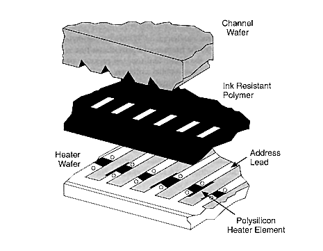
Figure 1
Xerox Corporation's Thermal Inkjet (TIJ) printhead implementation. Source: Xerox Corp.
Business Challenges
The large-market was "bootstrapped" in this case by the introduction of color printers with unprecedented performance/cost ratios. MEMS technology was the enabler for the product that created the large volume market required to sustain the MEMS investment. The market volume has been further sustained over time because the TIJ printheads are disposable—that is, the MEMS components are embedded in consumable supplies. Time to market is typically not excessive in these applications, because TIJ heater wafers can be piggybacked readily on slightly modified baseline MOS processes and because the fluid-flow pathways are relatively uncomplicated micromachined parts. In addition, the first-order coupling between domains (electrical-thermal-fluid dynamics) is fairly well understood in this case, and mature thermofluidic simulation tools are commercially available. The MEMS-specific infrastructure investment can stay moderate because the application does not demand state-of-the-art linewidths or feature sizes. Depreciated process lines can be revived and can deliver another life-cycle of perfectly acceptable service.
Technical Challenges
Important material-related challenges in TIJ are cavitation and corrosion. Without cavitation protection, the lifetime of a polysilicon film is very limited when the film is exposed to the cyclic and focused pressure pulses of up to 100 atm that occur during vapor bubble collapse. A Tantalum barrier is deposited over the polyheaters for cavitation protection. Other customizations of the heater wafer baseline process satisfy requirements of thermal efficiency, heater stability, and protection from the ionic ink environment. Thermal efficiency is achieved through a thicker-than-usual field oxide to avoid thermal losses to the substrate, and the MOS circuitry is protected from the ionic ink environment with an extra polyimide passivation film. The ink cartridge (i.e., packaging) is typically the cost-dominating factor in disposable TIJ printheads. One approach to reduce packaging/interconnect expense is to integrate addressing and multiplexing logic onto the ejector die to minimize the external lead count.
Acknowledgments
The presented Xerox TIJ printheads were developed through the joint efforts of J. Becerra, C. Burke, N. Deshpande, D. Drake, A. Fisher, B. Hawkins, D. Ims, G. Kneezel, J. Kubby, M. O'Horo, J. O'Neill, T. Orlowski, R. Proano, I. Rezanka, T. Tellier, S. Vandebroek, I. Vitomirov, and many other members of the Xerox Wilson Center for Research and Technology and the Xerox Advanced Imaging Business Unit, Webster, New York.
References
Courtney, T., R. E. Drews, V. J. Hull, D. R. Ims, and M. P. O'Horo. 1994. Print element for Xerox thermal ink jet print cartridge. Color Hard Copy and Graphics Arts III Conference, May 1994. SPIE Proceedings 2171:126-130.
Petersen, K. E. 1982. Silicon as a mechanical material. Proceedings of IEEE 70(5):420-457.
Walsh, S., B. Carr, H. Mados, and D. Narang. 1996. Commercializing MEMS--Too fast or too slow? Micromachined Devices and Components II Conference, September 1996. SPIE Proceedings 2882:12-17.


