
6
Slicing and Alloying Halide Perovskites
Following Ramamoorthy Ramesh, Hemamala Karunadasa of Stanford University continued by describing systems that might be used to create new moiré quantum materials. Karunadasa, a synthetic chemist, described halide perovskites and how single layers of those materials can be created and put to use in creating new materials with interesting properties. She began by talking about the optical, electronic, and structural diversity of the halide perovskites and then offered two case studies that show the potential of these materials in the field of moiré lattice systems.
CREATING HALIDE PEROVSKITE STRUCTURES
Noting that Ramesh had offered an introduction to oxide perovskites, Karunadasa explained that replacing the oxide with a halide would produce halide perovskites. The two types of perovskites have similar structures, but there is a major difference in what it takes to create them. “Oxide perovskites are forged in a furnace at around 1500 degrees over the course of a few days,” she said. “In contrast, halide perovskites self-assemble at room temperature in solution—in organic solvents, even in water.”
Furthermore, she added, because the halide perovskites are created at such low temperatures, it is possible to stuff small organic molecules into the cavities of the material (see Figure 6-1A). If the organic molecule is too large, it can lead to the splitting apart of the perovskite layers and creation of two-dimensional perovskites containing the organic molecules, a process called “dimensional re-
duction” (see Figure 6-1B). These constructs, with single two-dimensional layers of perovskite flanked by layers of organic molecules, were the focus of the next part of her talk.
For her, Karunadasa said, the most compelling aspect of these materials is how they are formed: “We take a pot of water, and we throw all the precursors into the solution. You can imagine, in solution there is this crazy free for all with organic molecules and inorganic ions tumbling around in solution, and our job as synthetic chemists is to figure out the conditions under which this mess, on its own accord, chooses to form these elaborate structures.” Through a great deal of experimentation with different materials, she said, one learns that there are certain organic molecules that allow for templating of specific inorganic architectures and, likewise, there are certain inorganic architectures that allow for templating of specific organic molecules.
The challenge of solution-state self-assembly is to try to get the molecules and the ions to form the desired structure “because it will do whatever it wants,” she said. The beauty of solution-state self-assembly is that once you have identified the conditions under which a particular material forms, it is possible to reproduce the material on demand with atomically smooth organic—inorganic interfaces in a scalable manner. The resulting material can be in the form of thin films, large single crystals, or polycrystalline powders.
In these constructs, Karunadasa noted, there are two pieces that can be manipulated—the organic layers and the inorganic layers—and she offered a number of
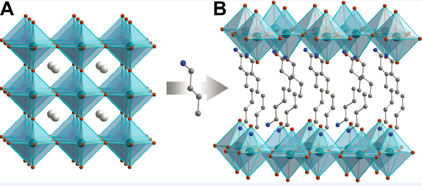
SOURCE: Hemamala Karunadasa, Stanford University, presentation to the workshop, May 19, 2021; used with permission from Annual Reviews, Inc., from M.D. Smith, E.J. Crace, A. Jaffe, and H.I. Karunadasa, 2018, “The Diversity of Layered Halide Perovskites,” Annual Review of Materials Research 48:111–136, permission conveyed through Copyright Clearance Center, Inc.
examples of these constructs to provide an idea of the types of things that can be built in this manner. She began with several examples of organic layers that have been attached to perovskites.
Both small-molecule intercalation and small-molecule reactivity have been seen with these materials (Smith et al. 2017). That is somewhat surprising, she said, because they are completely non-porous. “And yet they expand like an accordion to accommodate small molecule guests.” As an example she showed a two-dimensional perovskite that could expand to accept large numbers of iodine molecules via intercalation and a second that accepted iodine via reactivity. That second material was developed, she said, to capture radioactive iodine gas emitted from nuclear power plants. In another example, monomers were placed between the perovskite sheets and hit with gamma radiation which created one-dimensional polymers between the perovskite layers
In short, she said, it is possible to do all sorts of tricks with the organic layers, but in terms of the electronic properties, the inorganic components are much more important. So she offered some examples of the sorts of electronic structures that can be formed depending on how the three-dimensional perovskite is conceptually sliced to form two-dimensional perovskites. For instance, slicing very thinly diagonally through a three-dimensional perovskite forms a sort of corrugated two-dimensional perovskite, which absorbs ultraviolet light but emits white light. Its electronic structure is highly localized, and excitons get trapped in the lattice (Dohner et al. 2014). By contrast, slicing horizontally across the perovskite to get several layers together produces a material that absorbs sunlight and produces electrical current (Smith et al. 2014).
PROPERTIES OF HALIDE PEROVSKITES
Next Karunadasa described some of the variety exhibited by halide perovskites in their optical and electronic properties (Smith et al. 2018). For example, layered halide perovskites (i.e., materials with perovskite layers interspersed with organic layers) can be tuned to luminesce in almost any color—purple, blue, green, orange, red, white, near infrared, and so on (Smith et al. 2019).
In terms of bandgaps, she continued, there is a wide variety of bandgaps that one can choose from in perovskites. She discussed three types of these bandgaps in particular: ligand-to-metal charge transfer, metal-to-metal charge transfer, and inorganic-to-organic charge transfer. Ligand-to-metal charge transfer can be found in two-dimensional copper-halide perovskites such as R2CuCl4 or R2CuBr4, where R is a 1+ organic ion, or three-dimensional double perovskites with vacancies such as Cs2SnI6. The presence of metal-to-metal charge transfer is intriguing, she said, because it makes it possible to change the bandgap by choosing the metal combination. Examples include three-dimensional double perovskites such as Cs2AgTlBr6
and two-dimensional mixed-valence perovskites such as R4Cu(CuIn)0.5Cl8 where R is a 1+ organic ion and the copper atoms are copper 1+ and copper 2+. In the third case, she said, inorganic-to-organic charge transfer requires organic molecules with low-energy orbitals, and these molecules tend to be a little too large to fit into a three-dimensional perovskite, so to get such a structure Karunadasa’s group used an “expanded analog of a perovskite” where each octahedron is replaced with an edge-sharing dimer of octahedra that still connect through shared corners and that provide larger cavities that can hold aromatic organic molecules with low-energy pi orbitals (Umeyama et al. 2020).
Karunadasa then spoke about the electron transport properties of these halide perovskite structures. All halide perovskites are insulators or semiconductors, with bandgaps greater than about 1 eV, she said, although the bandgap can be closed at very high pressures, on the order of 50–60 GPa, for certain perovskites. Metallic transport can be created in some perovskites, such as three-dimensional tin-iodine perovskites, through hole doping. On the other hand, some halide perovskites will spontaneously lose halogen gas, such as bromine gas, leading to electron doping and increased conductivity; in the case of three-dimensional Cs2AgTlBr6, once the bromine gas has escaped, it can be replaced by putting the material in a bromine atmosphere for a week or so. “We are quite interested in trying to control this halogen degassing reaction,” Karunadasa said, “because we think it is a powerful way of doping these materials to the point where we can get decent transport properties.”
The Uses of Impurities in Double Perovskites
Homovalent and heterovalent impurities can produce dramatic changes in the optical and electronic properties of two-dimensional and three-dimensional halide perovskites, Karunadasa said, and she offered an example of each.
Concerning three-dimensional halide perovskites, she said that these materials have been known since the 1800s, but they have received rapidly increasing interest over the past decade and a half because of the fact that lead-halide perovskites have exceptional properties as photovoltaic absorbers. Between 2009 and 2015, the efficiency of these materials in absorbing sunlight and transforming it into electric current increased from around 4 percent to approximately 20 percent—a huge jump in a short period of time. However, these materials have various issues. Most concerning, it is a water soluble lead salt which is not particularly stable to moisture or heat, so the potential release of lead from these materials would be a major disadvantage in any commercial application. So there is a great deal of interest in finding less toxic and more stable analogues as the next-generation absorbers.
Thus Karunadasa’s group has been trying to determine how to find a three-dimensional perovskite that is lead-free but has similar photovoltaic properties. “We have concluded that no one metal can do it [take the place of the lead in the
perovskite],” she said, “but perhaps a mixture of two metals could.” The typical perovskite structure—AIBIIX3—requires a 2+ B-site metal, but the candidates are not satisfactory, so her team is looking at double perovskites with an AI2BB'X6 structure where the two metals, B and B', alternate in the three-dimensional lattice. This provides much more flexibility since in a single perovskite the octahedron metal has to be a 2+, but in a double perovskite the average charge of the octahedron site has to be 2+, but that can be distributed equally or unequally, so the charges could be 1+, 2+, 3+, 4+, or a vacancy (i.e., 0 charge), as long as the two choices average to 2+.
This provides many options—perhaps too many, she said. “Since we can work with pretty much any metal in the periodic table … how do we know which two metals will give us the properties we want with respect to photovoltaics?” she asked. “That is, how do we know which materials will give us the bandgap magnitude we want and the bandgap symmetry that we want?” It is particularly difficult because it is the combination of the two metals that will determine the properties of the material.
So her group has exerted considerable effort looking for a strategy to predict the bandgap properties for double perovskites with various combinations of metals. It turns out that there are some qualitative ways to at least get an idea of the size of the bandgap, Karunadasa said. This involves extrapolating from the various individual bands in the material to the individual molecular orbitals that form the bands and observing how close in energy the molecular orbitals are to one another; if they are inherently close together, they will form bands with a small bandgap, whereas if the molecular orbitals are father apart, they tend to form larger bandgaps. “This holds true for all the double perovskites we have looked at,” she said. This allows them to predict, to some extent, whether a bandgap will be large, medium, or small for a particular pairing of metals. This, combined with a second approach that she mentioned but did not describe, put her group in a good position to choose suitable candidates for B and B' in double perovskites for targeted bandgap energies and symmetry (direct/indirect gap), she said.
Working with the double perovskite material Cs2AgBiBr6, Karunadasa’s team found that they could tweak the band structure by adding small amounts—less than 1 atom percent—of thallium impurities. This affects the light-absorbing properties of the material, turning a normally translucent red crystal into an opaque black one with the same crystalline structure, and it also shifts the position of the bandgap, with the size of the bandgap decreasing with increasing levels of the impurity. In particular, with less than 1 percent thallium impurity, the indirect bandgap drops from nearly 2 eV to about 1.4 eV, she said, “which is exactly where you want to be for photovoltaics.” The thallium atoms seem to be replacing bismuth atoms in the lattice, and replacing all of the bismuth with thallium to create Cs2AgTlBr6 results in “the lowest bandgap I have seen in a halide perovskite,” she said, of about 0.95 eV.
Like lead, thallium is not an element that should be placed in large amounts in commercial products, so the next question to ask, Karunadasa said, is what the thallium did and whether another element could be found that would do something similar. In particular, she said, the question is, what other metals have empty 6s valence orbitals and can be accommodated in a perovskite lattice? Asking the question in that way points to Sn4+, which is isoelectric with Tl3+ and adopts the B site in perovskites with vacancies. It turns out that tin does the same thing in the Cs2AgBiBr6 perovskite as thallium, shifting both the bandgap and absorption. It is not immediately obvious which elements the tin substitutes for in the perovskite, she said, but her group’s studies found that Sn2+ substitutes for Ag1+ and Sn4+ substitutes for Bi3+, in both cases generating Ag1+ vacancies for charge compensation. The result is a large bandgap reduction that mimics the bandgap shift produced by thallium but without the problem of toxicity.
Alloying Single and Double Perovskites
This in turn led her group to begin thinking about impurity alignments, she said. Homovalent impurities can form a solid solution across most mixing ratios, such as A(SnxPb1–x)X3. By contrast, heterovalent impurities typically substitute effectively only when the impurity accounts for less than 1 percent of the atoms in the material; an example is Sn4+ impurities in Cs2AgBiBr6. The reason, Karunadasa explained, is that the impurities generally lead to a lattice mismatch, and a lattice cannot accommodate too many such mismatches. However, if one adds a large amount of the impurity, then it can lead to a new lattice structure in which all of the atoms fit comfortably.
In particular, her team has done this in alloying a single layered perovskite and a double layered perovskite to create a layered perovskite in which every metal is a mixed copper–indium site: (PCA)4[CuII(CuIInIII)0.5Cl8] (see Figure 6-2) (Connor et al. 2021). By creating such an alloy, one can get new properties, Karunadasa said. For instance, the alloyed material is black, while the single perovskite is bright yellow and the double perovskite is colorless. The reason the alloyed material is black is that it has strong low-energy absorption produced by intervalence charge transfer. This Cu(I/II) mixed valence is reminiscent of n-doped cuprate superconductors, which also have the Cu(I/II) couple in a similar square lattice, she said.
The Future of Two-Dimensional Perovskites
One can also carry out dimensional reduction on various double perovskites, Karunadasa said, and this reduction has various interesting consequences. In some double perovskites, for instance, reducing the dimensionality from a three-dimensional perovskite to a two-dimensional perovskite with single metal-halide
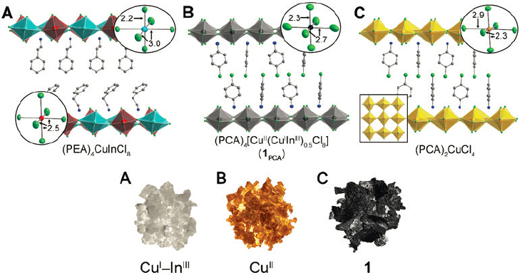
SOURCE: Hemamala Karunadasa, Stanford University, presentation to the workshop, May 19, 2021; used with permission from Royal Society of Chemistry, from B.A. Connor, R. Smaha, J. Li, et al., 2021, “Alloying a Single and a Double Perovskite: A Cu+/2+ Mixed-Valence Layered Halide Perovskite with Strong Optical Absorption,” Chemical Science 12:8689, permission conveyed through Copyright Clearance Center, Inc.
layers transforms the bandgap from indirect to direct, while in others the bandgap goes from direct to indirect when the dimensionality is similarly reduced. “So dimensional reduction is also a way to change the bandgap symmetry,” she said. This is similar to what happens when MoS2 is mechanically exfoliated to create two-dimensional structures; the bulk material has an indirect bandgap, while a single exfoliated flake has a direct bandgap. The difference is that with the perovskites, instead of exfoliation, organic molecules are used to separate the inorganic sublattices.
And, she said, wrapping up this portion of her presentation, there are many different types of two-dimensional perovskites with organic bilayers, with many different properties, that would be very amenable to exfoliation. “Basically any 2D perovskite with an organic bilayer will have very weak interactions between the organic layers,” she said, and these materials are known to cleave along the organic bilayers. The exfoliation can be done with single perovskites, double perovskites, and many others. “There is a huge phase space to explore.” Some recent papers have described exfoliating such materials all the way down to a monolayer, she said (Leng et al. 2018), adding that it is a fast-growing field.
A next step, she said, could be to take these single layers and stack them, perhaps with twists between the layers, to see what sorts of properties might emerge. This would represent a whole new family of materials that could be easily synthesized
in water, then exfoliated as sheets and stacked. “I’m excited to see what the halide perovskite homo- and heterostructures might have to offer us.”
THE POTENTIAL OF HALIDE PEROVSKITE HOMO- AND HETEROSTRUCTURES
In the last portion of her talk, Karunadasa described two recent studies that she said demonstrate this potential of halide perovskite home- and heterostructures.
The first was a theoretical study of bilayers of two-dimensional perovskites (Zhang et al. 2021). In particular, the researchers focused on the perovskite MA2PbI4, where MA is methylammonium, CH3NH3. The perovskite homo bilayer—that is, two sheets of MA2PbI4 held together with van der Waal forces—is analogous in several ways to the MoS2–WS2 hetero bilayer structure, such as the interlayer distances between the various atoms in the two structures. The researchers calculated the band structure of the Pb–I bilayer and found that the rotation of the CH3NH3 groups can considerably change the charge distribution. This is a new parameter that can be tuned in these materials, she said.
When they calculated the consequences of twisting the two Pb–I layers, the researchers found that the valence band flattens at an angle of 8.1°. The researchers argued that the reason the valence band flattens is that it has electronic states from both the top and bottom layers, so it is much more sensitive to the twist angle. By contrast, the conduction band has electronic states primarily from the bottom layer, and it does not flatten. This is also the case for MoS2–WS2, she said.
This is a very exciting theoretical study, Karunadasa said, and it indicates that researchers should try to create such perovskite bilayers.
She concluded by describing what she said she hopes is a complementary study that her group has carried out on the self-assembly of heterostructures (see Figure 6-3). Recently, she said, her group has figured out how to use organic molecules to direct the assembly of a bulk heterostructure that consists of alternating layers of halide perovskite and non-perovskite interfaces (Aubrey et al. 2021). There are two important features of this approach. First, because organic groups are used to direct the self-assembly, modifying the organic molecules changes the heterostructure that will crystallize, she said, “and we think this method is infinitely tunable to form various different intergrowths between the perovskites.” Furthermore, these materials form as single crystals, so single-crystal X-ray diffraction can be used to determine the structure of the crystals very precisely.
To date, she said, her group has synthesized at least nine of these heterostructures. In general they consist of repeating layers of perovskite, organic layer, intergrowth, and organic layer. In one such case, the perovskite and the intergrowth are connected. Here, the perovskite forms the conduction band, while intergrowth
SOURCE: Hemamala Karunadasa, Stanford University, presentation to the workshop, May 19, 2021; reprinted with permission from Springer Nature: M.L. Aubrey, A. Saldivar Valdes, M.R. Filip, et al., 2021, “Directed Assembly of Layered Perovskite Heterostructures as Single Crystals,” Nature 597:355, © 2021.
forms the valence band. The intergrowth also changes the dispersion of the conduction band by straining the perovskite lattice, Karunadasa said. Optical excitation delocalizes charge between both perovskite and intergrowth layers.
Summing up, she said that the theoretical paper motivates the search for bilayer homo- and heterostructures made out of perovskites, while her group’s synthesis work offers hope that the self-assembly of halide perovskite heterostructures as single crystals may offer a path for realizing the exotic properties of hetero bilayer interfaces in bulk materials that form in water.
QUESTION-AND-ANSWER SESSION
In a brief period following her presentation, which was moderated by Aharon Kapitulnik, Karunadasa answered several questions about her work. The first question was about the role of seeds or growth surfaces in growing the perovskite materials in solution. Seeds are very helpful for growing very large crystals, she replied, and her group routinely uses seed crystal if they want crystals on the order of centimeters. Their standard protocol is to filter out any tiny particles from the solutions and grow perovskites crystals just from a homogeneous mixture, but then these crystals can be used as seeds. Perovskites can be grown on top of other perovskites as well, she said, even those with a different composition.
Responding to a question about how her group measured conductivity in the halide perovskites, Karunadasa said the best way was to grow large enough single crystals that electrodes can be place along the sheets, although one must be careful with the choice of electrodes. The only electrode material that does not react with the halide perovskites is carbon, she said. If it is not possible to grow large enough
single crystals, multi-crystalline pellets can be used, but then any conductivity measurement is only a lower limit. Finally, various spectroscopies can be used to get a measure of conductivity.
Kapitulnik asked whether these halide perovskite materials with organic layers interspersed between the perovskite layers might have enough flexibility to be compressed or twisted as a way of modifying their electronic properties. That is definitely worth looking at, Karunadasa replied. As far as she knows, she said, no one has tried putting a torque on these materials to create twist angles between the layers. As for compressing, she said, there has been a lot of work on the high-pressure properties of perovskites, and the material gives in other ways before the organic layer finally starts to buckle.
In response to a question about the stability of halide perovskites, Karunadasa said that it is the lead halide perovskites that are most sensitive to moisture and heat, while most are stable in the presence of those factors—although they cannot, of course, be placed directly in water because they are ionic salts. The double perovskites also are generally stable, particularly the chlorides and bromides, while the iodides tend to be more sensitive to moisture and even light in some cases. Generally speaking, she said, there is a huge diversity in these materials’ stability, but it is typically possible to find stable examples.
REFERENCES
Aubrey, M.L., A.S. Valdes, M.R. Filip, B.A. Connor, K.P. Lindquist, J.B. Neaton, and H.I. Karunadasa. 2021. “Directed Assembly of Layered Perovskite Heterostructures as Single Crystals.” Nature 597:355–359.
Connor, B.A., R.W. Smaha, J. Li, A. Gold-Parker, A.J. Heyer, M.F. Toney, Y.S. Lee, and H.I. Karunadasa. 2021. “Alloying a Single and a Double Perovskite: A Cu+/2+ Mixed-Valence Layered Halide Perovskite with Strong Optical Absorption.” Chemical Science 12:8689–8697.
Dohner, E.R., E.T. Hoke, and H.I. Karunadasa. 2014. “Self-Assembly of Broadband White-Light Emitters.” Journal of the American Chemical Society 136(5):1718–1721.
Leng, K., I. Abdelwahab, I. Verzhbitskiy, M. Telychko, L. Chu, W. Fu, X. Chi, N. Guo, Z. Chen, Z. Chen, et al. 2018. “Molecularly Thin Two-Dimensional Hybrid Perovskites with Tunable Optoelectronic Properties Due to Reversible Surface Relaxation.” Nature Materials 17:908–914.
Smith, I.C., E.T. Hoke, D. Solis-Ibarra, M.D. McGehee, and H.I. Karunadasa. 2014. “A Layered Hybrid Perovskite Solar-Cell Absorber with Enhanced Moisture Stability.” Angewandte Chemie International Edition 53(42):11232–11235.
Smith, I.C., M.D. Smith, A. Jaffe, Y. Lin, and H.I. Karunadasa. 2017. “Between the Sheets: Postsynthetic Transformations in Hybrid Perovskites.” Chemistry of Materials 29(5):1868–1884.
Smith, M.D., E.J. Crace, A. Jaffe, and H.I. Karunadasa. 2018. “The Diversity of Layered Halite Perovskites.” Annual Review of Materials Research 48:111–136.
Smith, M.D., B.A. Connor, and H.I. Karunadasa. 2019. “Tuning the Luminescence of Layered Halite Perovskites.” Chemical Reviews 119(5):3104–3139.
Umeyama, D., L. Leppert, B.A. Connor, M.A. Manumpil, J.B. Neaton, and H.I. Karunadasa. 2020. “Expanded Analogs of Three-Dimensional Lead-Halide Hybrid Perovskites.” Angewandte Chemie International Edition 59(43):19087–19094.
Zhang, L., X. Zhang, and G. Lu. 2021. “Predictions of Moiré Excitons in Twisted Two-Dimensional Organic–Inorganic Halide Perovskites.” Chemical Science 12:6073–6080.


